EUV Lithography Equipment Manufacturing in 2025: The Critical Engine Driving Semiconductor Innovation. Explore Market Growth, Disruptive Technologies, and Strategic Outlook for the Next Five Years.
- Executive Summary: Key Findings and Market Highlights
- Market Overview: EUV Lithography Equipment in 2025
- Growth Forecast 2025–2030: Market Size, CAGR, and Revenue Projections
- Competitive Landscape: Leading Players, Market Shares, and Strategic Moves
- Technology Deep Dive: EUV Lithography Innovations and Roadmap
- Supply Chain Analysis: Challenges, Opportunities, and Geopolitical Impacts
- End-User Demand: Semiconductor Manufacturers and Application Trends
- Investment & M&A Activity: Funding, Partnerships, and Consolidation
- Regulatory Environment and Policy Impacts
- Future Outlook: Disruptive Trends, Risks, and Strategic Recommendations
- Sources & References
Executive Summary: Key Findings and Market Highlights
The global market for Extreme Ultraviolet (EUV) lithography equipment is poised for robust growth in 2025, driven by escalating demand for advanced semiconductor devices and the ongoing transition to sub-7nm process nodes. EUV lithography, a technology that utilizes extremely short wavelengths (13.5 nm) to etch intricate patterns onto silicon wafers, is now a critical enabler for next-generation integrated circuits. The market is characterized by high entry barriers, significant capital investment, and a concentrated supplier landscape.
Key findings indicate that ASML Holding N.V. remains the sole commercial supplier of EUV lithography systems, maintaining a near-monopoly due to its technological leadership and extensive intellectual property portfolio. In 2025, ASML’s latest EUV platforms, such as the Twinscan NXE and EXE series, are expected to see increased adoption among leading foundries and integrated device manufacturers (IDMs), including Taiwan Semiconductor Manufacturing Company Limited and Samsung Electronics Co., Ltd.. These companies are leveraging EUV to produce chips for high-performance computing, artificial intelligence, and 5G applications.
The market is also witnessing significant investments in the EUV supply chain, particularly in the development of high-power light sources, advanced photoresists, and defect inspection tools. Key suppliers such as Carl Zeiss SMT GmbH (optics) and Cymer, LLC (light sources, a subsidiary of ASML) are critical to the ecosystem, ensuring the reliability and scalability of EUV technology.
Despite its promise, the EUV lithography market faces challenges, including high system costs (exceeding $150 million per unit), complex maintenance requirements, and the need for ultra-clean manufacturing environments. However, ongoing R&D efforts and collaborative initiatives among industry leaders are expected to drive further cost reductions and yield improvements.
In summary, 2025 will mark a pivotal year for EUV lithography equipment manufacturing, with expanding adoption across leading-edge semiconductor fabs, continued dominance by ASML Holding N.V., and a strengthening ecosystem of specialized suppliers. The technology’s evolution will be instrumental in sustaining Moore’s Law and enabling future innovations in the semiconductor industry.
Market Overview: EUV Lithography Equipment in 2025
The market for Extreme Ultraviolet (EUV) lithography equipment is poised for significant growth in 2025, driven by the ongoing demand for advanced semiconductor manufacturing technologies. EUV lithography, which utilizes light with a wavelength of 13.5 nanometers, enables the production of smaller, more powerful, and energy-efficient chips, essential for applications in artificial intelligence, 5G, and high-performance computing. The transition to EUV is a critical step for semiconductor manufacturers aiming to maintain Moore’s Law and meet the increasing complexity of integrated circuits.
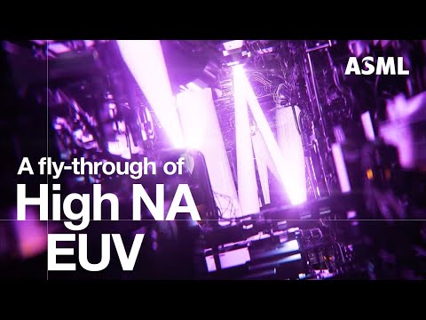
In 2025, the EUV lithography equipment market remains highly concentrated, with ASML Holding N.V. as the sole supplier of commercial EUV systems. ASML’s EUV machines are integral to the production of leading-edge chips at 5nm, 3nm, and the emerging 2nm nodes. The company’s continued innovation, including the rollout of its High-NA (Numerical Aperture) EUV systems, is expected to further enhance resolution and productivity, solidifying its dominance in the sector.
The primary customers for EUV lithography equipment are major foundries and integrated device manufacturers (IDMs), such as Taiwan Semiconductor Manufacturing Company Limited, Samsung Electronics Co., Ltd., and Intel Corporation. These companies are investing heavily in EUV technology to maintain their competitive edge and to support the production of next-generation chips for consumer electronics, automotive, and data center applications.
Geopolitical factors and export controls continue to shape the market landscape in 2025. Restrictions on the sale of advanced EUV systems to certain regions, particularly China, have influenced global supply chains and investment strategies. Meanwhile, governments in the United States, Europe, and Asia are increasing support for domestic semiconductor manufacturing, further fueling demand for EUV equipment.
Despite the high cost and technical complexity of EUV lithography systems, the market outlook for 2025 is robust. The ongoing miniaturization of semiconductor devices, coupled with the proliferation of advanced technologies, ensures that EUV lithography equipment will remain a cornerstone of the semiconductor industry’s evolution in the coming years.
Growth Forecast 2025–2030: Market Size, CAGR, and Revenue Projections
The EUV (Extreme Ultraviolet) lithography equipment manufacturing sector is poised for robust growth between 2025 and 2030, driven by escalating demand for advanced semiconductor devices and the ongoing transition to sub-5nm process nodes. Industry analysts anticipate a compound annual growth rate (CAGR) in the range of 12% to 15% during this period, with the global market size projected to surpass $30 billion by 2030. This expansion is underpinned by the increasing adoption of EUV technology by leading foundries and integrated device manufacturers (IDMs), who are seeking to maintain Moore’s Law and deliver higher performance, lower power chips for applications such as artificial intelligence, 5G, and high-performance computing.
The market’s growth trajectory is largely shaped by the technological leadership of ASML Holding N.V., the sole supplier of commercial EUV lithography systems. ASML’s ongoing investments in R&D and capacity expansion are expected to alleviate supply constraints and enable higher shipment volumes from 2025 onwards. Additionally, the company’s introduction of next-generation High-NA (Numerical Aperture) EUV systems is anticipated to further accelerate market growth by enabling even smaller feature sizes and improved yield for semiconductor manufacturers.
Geographically, the Asia-Pacific region—particularly Taiwan, South Korea, and China—will continue to dominate EUV equipment demand, fueled by aggressive fab expansions from major players such as Taiwan Semiconductor Manufacturing Company Limited and Samsung Electronics Co., Ltd.. Meanwhile, the United States and Europe are expected to increase their investments in domestic semiconductor manufacturing, supported by government initiatives and funding programs aimed at strengthening supply chain resilience.
Revenue projections for the period reflect not only the rising unit sales of EUV scanners but also the growing market for related subsystems, service contracts, and upgrades. As the ecosystem matures, ancillary suppliers—such as Carl Zeiss SMT GmbH (optics) and Cymer LLC (light sources)—are expected to see parallel growth, further boosting the overall market value. In summary, the 2025–2030 outlook for EUV lithography equipment manufacturing is characterized by strong double-digit growth, technological innovation, and expanding global adoption.
Competitive Landscape: Leading Players, Market Shares, and Strategic Moves
The competitive landscape of EUV (Extreme Ultraviolet) lithography equipment manufacturing in 2025 is characterized by a high degree of concentration, technological complexity, and strategic maneuvering among a handful of global players. The market is overwhelmingly dominated by ASML Holding N.V., which remains the sole commercial supplier of EUV lithography systems worldwide. ASML’s EUV machines are critical for the production of advanced semiconductor nodes, and the company’s technological leadership is underpinned by its proprietary light source technology, precision optics, and extensive intellectual property portfolio.
ASML’s market share in EUV lithography equipment is estimated to exceed 90% in 2025, with its customers including leading semiconductor manufacturers such as Taiwan Semiconductor Manufacturing Company Limited (TSMC), Samsung Electronics Co., Ltd., and Intel Corporation. These companies rely on ASML’s EUV systems to fabricate cutting-edge chips at 5nm, 3nm, and beyond, cementing ASML’s pivotal role in the global semiconductor supply chain.
Despite ASML’s dominance, other players are making strategic moves to enter or influence the EUV ecosystem. Canon Inc. and Nikon Corporation, both established names in DUV (Deep Ultraviolet) lithography, have invested in research and development for next-generation lithography technologies, though they have yet to commercialize EUV systems. Meanwhile, suppliers such as Carl Zeiss AG (optics) and Cymer LLC (light sources, a subsidiary of ASML) play crucial roles in the EUV value chain, providing specialized components that are integral to system performance.
Strategically, ASML continues to invest heavily in R&D to improve throughput, yield, and cost efficiency of its EUV platforms, while also expanding its service and support infrastructure globally. The company is also navigating complex geopolitical dynamics, particularly export controls affecting shipments to China. Meanwhile, semiconductor manufacturers are forming strategic partnerships and consortia to secure access to EUV technology and drive process innovation. As the demand for advanced chips accelerates, the competitive landscape is expected to remain dynamic, with incremental innovation and supply chain resilience as key strategic priorities.
Technology Deep Dive: EUV Lithography Innovations and Roadmap
Extreme Ultraviolet (EUV) lithography has become the cornerstone technology for advanced semiconductor manufacturing, enabling the production of integrated circuits with features below 7 nanometers. The evolution of EUV lithography equipment is marked by significant innovations in optics, light sources, and system integration, driven primarily by the need for higher resolution, throughput, and yield in chip fabrication.
At the heart of EUV lithography systems are high-power light sources that generate 13.5 nm wavelength light, a feat achieved through laser-produced plasma (LPP) technology. The leading supplier, ASML Holding N.V., has pioneered the development of EUV scanners, integrating complex subsystems such as tin droplet targets, high-energy CO2 lasers, and sophisticated debris mitigation strategies to ensure stable and efficient EUV photon generation. The company’s latest EUV platforms, such as the NXE:3800E, are designed to deliver higher wafer throughput and improved overlay accuracy, critical for high-volume manufacturing in 2025 and beyond.
Optical systems in EUV lithography present unique challenges due to the absorption of EUV light by most materials, necessitating the use of multi-layered Bragg reflectors and ultra-precise mirrors. Carl Zeiss AG is a key partner in producing these mirrors, achieving surface precision at the atomic level to minimize aberrations and maximize reflectivity. The integration of these optics into the scanner requires advanced metrology and contamination control, as even minute particles can degrade performance.
The EUV roadmap for 2025 and beyond focuses on increasing source power, improving mask defectivity, and enabling High-NA (Numerical Aperture) systems. High-NA EUV, with a numerical aperture of 0.55 compared to the current 0.33, promises sub-2 nm patterning capabilities. ASML Holding N.V. has announced the EXE:5000 platform, targeting pilot production in 2025, which will require new resist materials, mask infrastructure, and further advances in system automation.
Collaboration across the supply chain is essential for EUV innovation. Intel Corporation, Taiwan Semiconductor Manufacturing Company Limited (TSMC), and Samsung Electronics Co., Ltd. are actively partnering with equipment manufacturers to co-develop process modules, drive yield improvements, and accelerate the adoption of next-generation EUV technology.
Supply Chain Analysis: Challenges, Opportunities, and Geopolitical Impacts
The supply chain for EUV (Extreme Ultraviolet) lithography equipment is among the most complex and tightly controlled in the global semiconductor industry. EUV systems, primarily produced by ASML Holding N.V., require thousands of highly specialized components sourced from a network of suppliers across Europe, the United States, and Asia. The manufacturing process involves precision optics from Carl Zeiss AG, high-power light sources, advanced mechatronics, and ultra-clean manufacturing environments. This intricate web creates both significant challenges and unique opportunities for stakeholders.
One of the main challenges is the extreme concentration of critical suppliers. For example, Zeiss is the sole provider of the high-precision mirrors essential for EUV systems, making the supply chain vulnerable to disruptions at any single point. Additionally, the need for ultrapure materials and components, such as specialized photoresists and pellicles, means that even minor quality or logistics issues can delay production. The COVID-19 pandemic and subsequent global chip shortages highlighted the fragility of these supply chains, prompting ASML Holding N.V. and its partners to invest in supply chain resilience and redundancy.
Opportunities arise from the growing demand for advanced semiconductors, which is driving investment in new manufacturing capacity and supply chain localization. Governments in the U.S., EU, and Asia are offering incentives to attract EUV-related manufacturing and research, aiming to reduce reliance on single regions or suppliers. This trend is fostering innovation among component manufacturers and encouraging the development of alternative suppliers for critical parts, such as optics and light sources.
Geopolitical factors have a profound impact on the EUV supply chain. Export controls imposed by the U.S. and the Netherlands restrict the sale of EUV systems and certain components to China, affecting global market dynamics and prompting Chinese firms to accelerate domestic R&D efforts. Meanwhile, trade tensions and regulatory scrutiny are leading companies like ASML Holding N.V. to diversify their supplier base and production locations. The interplay between technological leadership, national security concerns, and global competition will continue to shape the EUV lithography equipment supply chain in 2025 and beyond.
End-User Demand: Semiconductor Manufacturers and Application Trends
In 2025, end-user demand for EUV (Extreme Ultraviolet) lithography equipment is being driven by the semiconductor industry’s relentless pursuit of smaller, more powerful, and energy-efficient chips. Leading semiconductor manufacturers, such as Taiwan Semiconductor Manufacturing Company Limited (TSMC), Samsung Electronics Co., Ltd., and Intel Corporation, are at the forefront of adopting EUV lithography to enable advanced process nodes at 5nm, 3nm, and beyond. These companies are investing heavily in EUV tools to maintain technological leadership and meet the surging demand for high-performance computing, artificial intelligence, and 5G applications.
The application trends in 2025 reflect a broadening of EUV lithography’s role beyond high-end logic chips. Memory manufacturers, such as Micron Technology, Inc. and SK hynix Inc., are increasingly integrating EUV into DRAM and NAND flash production to achieve higher densities and lower power consumption. The automotive sector, driven by the proliferation of advanced driver-assistance systems (ADAS) and electric vehicles, is also emerging as a significant end-user, requiring chips with greater complexity and reliability.
The demand for EUV lithography equipment is further amplified by the growing need for chiplet architectures and heterogeneous integration, which require precise patterning at advanced nodes. This trend is prompting foundries and integrated device manufacturers (IDMs) to expand their EUV toolsets and invest in next-generation EUV systems with higher numerical apertures (High-NA EUV), as developed by ASML Holding N.V., the sole supplier of EUV lithography machines.
In summary, the end-user demand for EUV lithography equipment in 2025 is characterized by robust investments from leading semiconductor manufacturers, diversification into memory and automotive applications, and a focus on enabling next-generation chip designs. These trends underscore the central role of EUV technology in shaping the future of semiconductor manufacturing and driving innovation across multiple industries.
Investment & M&A Activity: Funding, Partnerships, and Consolidation
The EUV (Extreme Ultraviolet) lithography equipment manufacturing sector has witnessed significant investment and M&A activity in 2025, reflecting its critical role in the semiconductor value chain. As chipmakers push toward sub-5nm process nodes, demand for advanced EUV systems has surged, prompting both established players and new entrants to seek capital, forge partnerships, and pursue consolidation.
Funding: The capital-intensive nature of EUV technology has led to substantial funding rounds, particularly for suppliers of key subsystems such as light sources, optics, and metrology tools. ASML Holding NV, the dominant EUV system manufacturer, has continued to invest heavily in R&D, supported by robust cash flows and strategic government incentives from the European Union and the Netherlands. Meanwhile, component suppliers have attracted venture capital and strategic investments to scale up production and meet the stringent quality requirements of EUV systems.
Partnerships: Collaboration remains a cornerstone of EUV ecosystem development. In 2025, ASML Holding NV has deepened its partnerships with leading chipmakers such as Taiwan Semiconductor Manufacturing Company Limited (TSMC), Samsung Electronics Co., Ltd., and Intel Corporation to co-develop next-generation EUV platforms and process enhancements. Additionally, alliances with optics specialists like Carl Zeiss AG and light source providers have been strengthened to address technical bottlenecks and accelerate innovation.
Consolidation: The high barriers to entry and the need for integrated solutions have driven consolidation among subsystem suppliers and service providers. In 2025, several mergers and acquisitions have been announced, particularly in the fields of EUV mask inspection, pellicle manufacturing, and resist materials. These moves aim to streamline supply chains, enhance technological capabilities, and ensure the reliability of critical EUV components. The consolidation trend is also supported by strategic investments from major semiconductor foundries, seeking to secure access to key technologies and mitigate supply risks.
Overall, the investment and M&A landscape in EUV lithography equipment manufacturing in 2025 is characterized by robust funding, strategic partnerships, and targeted consolidation, all aimed at sustaining the rapid pace of innovation and meeting the escalating demands of advanced semiconductor production.
Regulatory Environment and Policy Impacts
The regulatory environment and policy landscape play a pivotal role in shaping the global market for EUV (Extreme Ultraviolet) lithography equipment manufacturing, particularly as the technology becomes central to advanced semiconductor production. In 2025, the sector is heavily influenced by export controls, intellectual property regulations, and international trade policies, especially among the United States, the European Union, Japan, South Korea, and China.
A key regulatory factor is the export control regime led by the U.S. Department of Commerce Bureau of Industry and Security and supported by allied nations. These controls restrict the sale of advanced EUV lithography systems and critical components to certain countries, most notably China, citing national security and technological leadership concerns. The Netherlands, home to ASML Holding N.V.—the world’s sole supplier of commercial EUV lithography machines—has implemented licensing requirements for the export of its most advanced systems, in alignment with U.S. policy and under pressure from international partners.
The European Union, through its European Commission, also enforces strict dual-use regulations, ensuring that sensitive technologies like EUV lithography are not diverted for unauthorized military or strategic uses. These policies are periodically updated to reflect technological advancements and geopolitical shifts, impacting the ability of manufacturers to access global markets.
Intellectual property (IP) protection is another critical regulatory aspect. The complexity and high R&D investment in EUV technology necessitate robust IP frameworks. Organizations such as the European Patent Office and the United States Patent and Trademark Office play a significant role in safeguarding innovations, which is essential for maintaining competitive advantage and encouraging further investment in the sector.
Additionally, environmental and safety regulations, such as those enforced by the European Chemicals Agency and national equivalents, govern the use of hazardous materials and energy consumption in EUV equipment manufacturing. Compliance with these standards is mandatory and can influence production costs and timelines.
Overall, the regulatory and policy environment in 2025 is characterized by heightened scrutiny, strategic export controls, and evolving compliance requirements, all of which significantly impact the global supply chain, market access, and innovation trajectory of EUV lithography equipment manufacturing.
Future Outlook: Disruptive Trends, Risks, and Strategic Recommendations
The future of EUV (Extreme Ultraviolet) lithography equipment manufacturing is shaped by a convergence of disruptive trends, emerging risks, and the need for strategic adaptation. As the semiconductor industry pushes toward sub-2nm process nodes, EUV lithography remains indispensable for enabling further miniaturization and performance gains. However, the sector faces both opportunities and challenges that will define its trajectory through 2025 and beyond.
One of the most significant disruptive trends is the increasing demand for High-NA (Numerical Aperture) EUV systems, which promise higher resolution and throughput. ASML Holding N.V., the sole supplier of EUV lithography systems, is leading the development of High-NA platforms, with pilot systems expected to be delivered to major chipmakers such as Intel Corporation and Taiwan Semiconductor Manufacturing Company Limited in 2025. These advancements are expected to accelerate the adoption of EUV in logic and memory manufacturing, but they also introduce new complexities in optics, mask technology, and process control.
Supply chain risks remain a critical concern. The EUV ecosystem relies on a highly specialized network of suppliers for components such as light sources, mirrors, and photoresists. Geopolitical tensions, export controls, and the concentration of key suppliers—such as Carl Zeiss AG for optics—pose potential bottlenecks. Additionally, the high cost and technical barriers to entry limit the number of players capable of producing EUV tools, increasing vulnerability to disruptions.
Environmental and energy considerations are also gaining prominence. EUV systems consume significant power and require advanced cleanroom environments, prompting manufacturers to invest in energy efficiency and sustainability initiatives. Regulatory pressures in Europe and Asia are likely to intensify, compelling equipment makers to innovate in both process and product design.
Strategic recommendations for stakeholders include diversifying the supplier base, investing in R&D for next-generation materials and process controls, and fostering closer collaboration across the value chain. Governments and industry bodies should support workforce development and cross-border research initiatives to mitigate talent shortages and accelerate innovation. For equipment manufacturers, maintaining technological leadership while ensuring supply chain resilience and environmental compliance will be key to sustaining growth in the evolving EUV landscape.
Sources & References
- ASML Holding N.V.
- Carl Zeiss SMT GmbH
- Canon Inc.
- Nikon Corporation
- Micron Technology, Inc.
- U.S. Department of Commerce Bureau of Industry and Security
- European Commission
- European Patent Office
- European Chemicals Agency